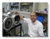
Suzuki, Motofumi
Professor: Motofumi Suzuki
Researches
He studies thin film nano-structures and -morphologies expecting the novel properties related them. Especially, he is now interested in the optical and mechanical properties of thin films with tailored nano-morphologies prepared by dynamic oblique deposition (DOD).

Contact:
Building C3, Room c2S10
Kyoto daigaku-Katsura, Nishikyo-ku
Kyoto 615-8540, Japan
TEL +81-75-383-3695 / FAX +81-75-383-3695
e-mail: m-snki@me
✴Add “.kyoto-u.ac.jp” after each e-mail address.
Education
1998
- Doctor of Engineering
- Kyoto University, Kyoto, JAPAN
Dissertation: Studies on the Giant Magnetoresistance in Magnetic Superlattices.
1988
- Master of Engineering
- Graduate School of Engineering, Kyoto University, Kyoto, JAPAN
Dissertation: Surface Structure of SnTe(001) and PbSe/SnTe(001) Studied by RBS/Channeling of MeV He+ Ions.
1986
- Bachelor of Engineering
- Faculty of Engineering, Kyoto University, Kyoto, JAPAN
Dissertation: Epitaxial Growth of Sputtered Ni Films on Alkali Halides.
Professional Experience
2013-
- Professor, Department of Micro Engineering, Graduate School of Engineering, Kyoto University, Kyoto, JAPAN.
2002-2013
- Associate Professor, Department of Engineering Physics and Mechanics, Graduate School of Engineering, Kyoto University, Kyoto, JAPAN.
- ・ Growth on nanowires by high temperature glancing angle deposition.
- ・ Development of spectrally-selective infra red thermal emitters.
- ・ Development of low reflectivity wire-grid polarizers.
- ・ Development of aligned nanorod arrays of noble metals and their applications to thin film polarizers, tunable plasmonic sensors and thermoplasmonics.
- ・ Investigations on initial stage of thin film growth of semiconducting silicides.
- ・ Development of rugate filters for optical communications.
- ・ Surface and interface analysis by using high resolution Rutherford backscattering spectroscopy.
- ・ Investigations of ion beam interaction with solid surfaces.
1988-2002
- Researcher, TOYOTA Central Research and Development Laboratories, Inc., Nagakute, Aichi 480-1192, JAPAN.
- ・ Development of integrated nanostructured thin films by dynamic oblique deposition.
- ・ Development of 3D thin film growth simulator VFiGS.
- ・ Development of thin-film waveplates of oblique columnar thin films for optical pickup.
- ・ Investigations on surface and interface properties of organic LED.
- ・ Investigations on the giant magentoresistance of metallic superlattices and their application to sensors.
- ・ Development of angular selective coatings containing metal nanoparticles.
